Samsung is launching the world's first three-dimensional NAND-memory
Samsung Electronics has announced the start of mass production of the industry's first NAND flash memory with a three-dimensional structure of the chip package and a vertical arrangement of the cells. New product allows, according to the company, to overcome the scalability limitations of existing non-volatile memory. 3D V-NAND with a favorable balance of performance and size will be applied in a wide range of consumer electronics and enterprise applications, including embedded NAND-memory and solid state drives (SSD).
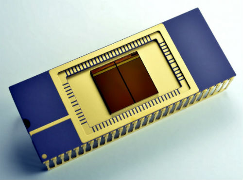
The first chip Samsung V-NAND capacity of 128 Gbps technology utilizes 3D Charge Trap Flash (CTF), which provides greater reliability and at the same time reduces the cost of flash memory chips compared to classical cell floating gate, as well as multi-layer technology layout with vertical connections vnutrichipovymi .
Over the past 40 years-in flash memory was created on the basis of flat-layer structures with cells floating-gate. However, after the development of the manufacturing process with the topological size of 10 nm scale there was a need for new technological solutions, since the interference between adjacent cells led to a decrease in reliability of NAND-memory. Attempts to solve the emerging problems in the framework of classical technologies entailed an increase in development time and the cost of the memory chips.
NEW V-NAND solve these technical problems, reaching a new level of development and production of NAND-memory chips through innovations in structure, circuit design and manufacturing process. To do this, Samsung has updated developed in 2006, the technology 3D Charge Trap Flash. In CTF-design electric charge (defining stored in the memory cell data) is temporarily placed in a special isolated area of the cell of a non-conductive silicon nitride (SiN) is used instead of classical technologies floating gate field-effect transistor to prevent interference between adjacent memory cells.
Due to the three dimensional structure of layers in CTF-design could greatly enhance the reliability and speed of the memory. New 3D V-NAND not only shows improved reliability from 2 to 10 times, but the recording speed increases twice as compared with the conventional NAND-memory with a floating gate made according to the process as 10-nm class.
In addition, one of the most important technological advances Samsung V-NAND is a vertical arrangement of the cells, which allows to connect up to 24 layers in a single chip memory. With this special etching technique allows creating a vertical conductive channels interconnecting layers from top to bottom. The new vertical structure will help Samsung to produce NAND flash memory higher capacity by increasing the number of 3D-layers of cells instead of further increasing chip area, resulting in a disproportionate increase in labor costs to manufacture it.


No comments: